- 您现在的位置:买卖IC网 > Sheet目录1227 > MAX1493EVKIT+ (Maxim Integrated Products)KIT EVAL FOR MAX1493
�� �
�
�3.5-� and� 4.5-Digit,� Single-Chip�
�ADCs� with� LCD� Drivers�
�Detailed� Description�
�The� MAX1491/MAX1493/MAX1495� low-power,� highly�
�integrated� ADCs� with� LCD� drivers� convert� a� ±2V� differ-�
�ential� input� voltage� (one� count� is� equal� to� 100μV� for� the�
�MAX1493/MAX1495� and� 1mV� for� the� MAX1491)� with� a�
�sigma-delta� ADC� and� output� the� result� to� an� LCD.� An�
�additional� ±200mV� input� range� (one� count� is� equal� to�
�10μV� for� the� MAX1493/MAX1495� and� 100μV� for� the�
�Digital� Filtering�
�The� MAX1491/MAX1493/MAX1495� contain� an� on-chip�
�digital� lowpass� filter� that� processes� the� data� stream�
�from� the� modulator� using� a� SINC4� (sinx/x)� 4� response.�
�The� SINC� 4� filter� has� a� settling� time� of� four� output� data�
�periods� (4� x� 200ms).�
�The� MAX1491/MAX1493/MAX1495� have� 25%� overrange�
�capability� built� into� the� modulator� and� digital� filter:�
�sin� ?� N� π�
�f� m� ?� ?� ?�
�?�
�f� ?� ??�
�sin� ?� π�
�?� f� m� ?� ?� ?�
�MAX1491)� is� available� to� measure� small� signals� with�
�increased� resolution.�
�These� devices� operate� from� a� single� 2.7V� to� 5.25V� power�
�supply� and� offer� 3.5-digit� (MAX1491)� or� 4.5-digit�
�(MAX1493/MAX1495)� conversion� results.� An� internal�
�2.048V� reference,� internal� charge� pump� and� a� high-accu-�
�?�
�?�
�H� (� f� )� =� ??�
�?�
�?� ?�
�1�
�N�
�?�
�?� f� ?� ?�
�?�
�?�
�4�
�(� )�
�?� 1� 1� -� z�
�(� )�
�?� N� 1� -� z�
�?�
�racy� on-chip� oscillator� eliminate� external� components.�
�These� devices� also� feature� on-chip� buffers� for� the� dif-�
�ferential� input� signal� and� external� reference� inputs,�
�allowing� direct� interface� with� high-impedance� signal�
�sources.� In� addition,� they� use� continuous� internal� offset�
�?� -N�
�H� (� z� )� =� ?� -� 1�
�?�
�?�
�?�
�?�
�?�
�4�
�calibration,� and� offer� >100dB� of� 50Hz� and� 60Hz� line�
�noise� rejection.� Other� features� include� data� hold� and�
�peak� hold,� and� a� low-battery� monitor.� The� MAX1495�
�also� performs� enhanced� offset� calibration� on� demand.�
�Analog� Input� Protection�
�Internal� protection� diodes� limit� the� analog� input� range�
�from� V� NEG� to� (AV� DD� +� 0.3V).� If� the� analog� input�
�exceeds� this� range,� limit� the� input� current� to� 10mA.�
�Internal� Analog� Input/�
�Reference� Buffers�
�The� MAX1491/MAX1493/MAX1495� analog� input/refer-�
�ence� buffers� allow� the� use� of� high-impedance� signal�
�sources.� The� input� buffers’� common-mode� input� range�
�allows� the� analog� inputs� and� reference� to� range� from�
�-2.2V� to� +2.2V.�
�Modulator�
�The� MAX1491/MAX1493/MAX1495� perform� analog-to-�
�digital� conversions� using� a� single-bit,� 3rd-order,� sigma-�
�delta� modulator.� The� sigma-delta� modulation� converts�
�the� input� signal� into� a� digital� pulse� train� whose� average�
�duty� cycle� represents� the� digitized� signal� information.�
�The� modulator� quantizes� the� input� signal� at� a� much�
�higher� sample� rate� than� the� bandwidth� of� the� input.�
�The� MAX1491/MAX1493/MAX1495� modulator� provides�
�3rd-order� frequency� shaping� of� the� quantization� noise�
�resulting� from� the� single-bit� quantizer.� The� modulator� is�
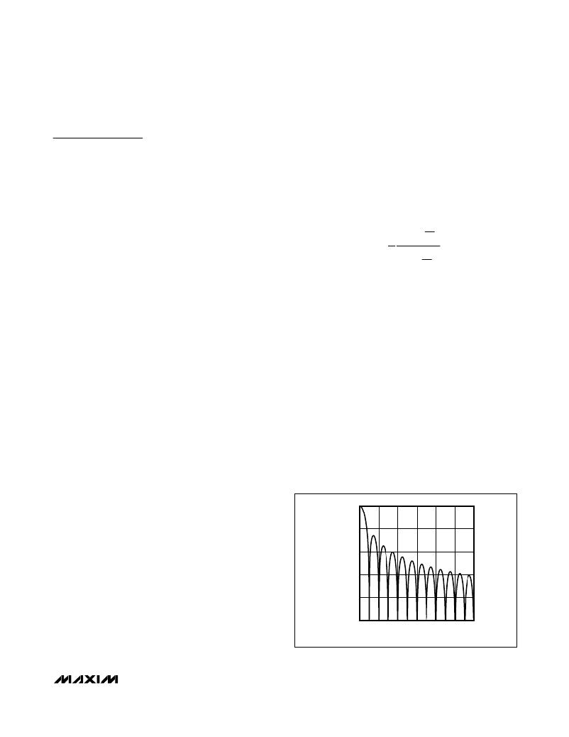
�Filter� Characteristics�
�Figure� 2� shows� the� filter� frequency� response.� The� SINC� 4�
�characteristic� -3dB� cutoff� frequency� is� 0.228� times� the�
�first� notch� frequency� (5Hz).� The� oversampling� ratio�
�(OSR)� for� the� MAX1491� is� 128� and� the� OSR� for� the�
�MAX1493/MAX1495� is� 1024.�
�The� output� data� rate� for� the� digital� filter� corresponds�
�with� the� positioning� of� the� first� notch� of� the� filter’s� fre-�
�quency� response.� The� notches� of� the� SINC� 4� filter� are�
�repeated� at� multiples� of� the� first� notch� frequency.� The�
�SINC� 4� filter� provides� an� attenuation� of� better� than�
�100dB� at� these� notches.� For� example,� 50Hz� is� equal� to�
�10� times� the� first� notch� frequency� and� 60Hz� is� equal� to�
�12� times� the� first� notch� frequency.�
�0�
�-40�
�-80�
�-120�
�-160�
�fully� differential� for� maximum� signal-to-noise� ratio� and�
�minimum� susceptibility� to� power-supply� noise.� A� single-�
�bit� data� stream� is� then� presented� to� the� digital� filter� for�
�-200�
�0�
�10�
�20� 30� 40�
�FREQUENCY� (Hz)�
�50�
�60�
�processing,� to� remove� the� frequency-shaped� quantiza-�
�tion� noise.�
�Figure� 2.� Frequency� Response� of� the� SINC� 4� Filter� (Notch� at� 60Hz)�
�_______________________________________________________________________________________�
�9�
�发布紧急采购,3分钟左右您将得到回复。
相关PDF资料
MAX16031EVKIT+
KIT EVALUATION FOR MAX1603
MAX16050EVKIT+
EVAL KIT FOR MAX16050
MAX16929EVKIT+
KIT EVALUATION FOR MAX16929
MAX16946EVKIT+
KIT EVALUATION FOR MAX16946
MAX17015EVKIT+
KIT EVAL FOR MAX17015
MAX17021EVKIT+
EVAL KIT FOR MAX17021
MAX1702EVKIT
EVAL KIT FOR MAX1702
MAX17710EVKIT#
RD ENERGY HARVESTING
相关代理商/技术参数
MAX1494CCJ
功能描述:模数转换器 - ADC RoHS:否 制造商:Texas Instruments 通道数量:2 结构:Sigma-Delta 转换速率:125 SPs to 8 KSPs 分辨率:24 bit 输入类型:Differential 信噪比:107 dB 接口类型:SPI 工作电源电压:1.7 V to 3.6 V, 2.7 V to 5.25 V 最大工作温度:+ 85 C 安装风格:SMD/SMT 封装 / 箱体:VQFN-32
MAX1494CCJ+
功能描述:模数转换器 - ADC 4.5 Digit ADC w/LCD Drivers RoHS:否 制造商:Texas Instruments 通道数量:2 结构:Sigma-Delta 转换速率:125 SPs to 8 KSPs 分辨率:24 bit 输入类型:Differential 信噪比:107 dB 接口类型:SPI 工作电源电压:1.7 V to 3.6 V, 2.7 V to 5.25 V 最大工作温度:+ 85 C 安装风格:SMD/SMT 封装 / 箱体:VQFN-32
MAX1494CCJ+T
功能描述:模数转换器 - ADC 4.5 Digit ADC w/LCD Drivers RoHS:否 制造商:Texas Instruments 通道数量:2 结构:Sigma-Delta 转换速率:125 SPs to 8 KSPs 分辨率:24 bit 输入类型:Differential 信噪比:107 dB 接口类型:SPI 工作电源电压:1.7 V to 3.6 V, 2.7 V to 5.25 V 最大工作温度:+ 85 C 安装风格:SMD/SMT 封装 / 箱体:VQFN-32
MAX1494CCJ-T
功能描述:模数转换器 - ADC RoHS:否 制造商:Texas Instruments 通道数量:2 结构:Sigma-Delta 转换速率:125 SPs to 8 KSPs 分辨率:24 bit 输入类型:Differential 信噪比:107 dB 接口类型:SPI 工作电源电压:1.7 V to 3.6 V, 2.7 V to 5.25 V 最大工作温度:+ 85 C 安装风格:SMD/SMT 封装 / 箱体:VQFN-32
MAX1494EVC16
功能描述:模数转换器 - ADC MAX1494C16 EVAL KIT RoHS:否 制造商:Texas Instruments 通道数量:2 结构:Sigma-Delta 转换速率:125 SPs to 8 KSPs 分辨率:24 bit 输入类型:Differential 信噪比:107 dB 接口类型:SPI 工作电源电压:1.7 V to 3.6 V, 2.7 V to 5.25 V 最大工作温度:+ 85 C 安装风格:SMD/SMT 封装 / 箱体:VQFN-32
MAX1494EVKIT
功能描述:数据转换 IC 开发工具 Evaluation Kit/Evaluation System for the MAX1493 MAX1494 MAX1495 RoHS:否 制造商:Texas Instruments 产品:Demonstration Kits 类型:ADC 工具用于评估:ADS130E08 接口类型:SPI 工作电源电压:- 6 V to + 6 V
MAX14950ACTL+
功能描述:外围驱动器与原件 - PCI PCIe Gen III Re-Driver RoHS:否 制造商:PLX Technology 工作电源电压: 最大工作温度: 安装风格:SMD/SMT 封装 / 箱体:FCBGA-1156 封装:Tray
MAX14950ACTL+T
功能描述:外围驱动器与原件 - PCI PCIe Gen III Re-Driver RoHS:否 制造商:PLX Technology 工作电源电压: 最大工作温度: 安装风格:SMD/SMT 封装 / 箱体:FCBGA-1156 封装:Tray